Why Designing PCBs Feels Fun and Easy to Me
A personal reflection on my PCB design journey, from hand-drawn marker layouts and toner-transfer boards in Pakistan to modern KiCad design and low-cost professional fabrication.
I first started designing printed circuit boards in 2011, when I was in Pakistan. At that time, PCB fabrication was not as easy or accessible as it is today. There were not many local fabrication facilities, and getting boards manufactured outside the country was not simple either. It really felt like the old days of electronics prototyping.
In the beginning, we used very simple DIY methods. Sometimes we would draw the PCB traces directly on a bare copper board using a permanent marker, place the board in etchant, drill the holes manually, and then solder the components by hand. It was simple, rough, and honestly very fun.
Later, we learned proper PCB design software and attended a workshop at NUST. My first PCB design instructor was Hamd ul Moqeet Riaz, he is in Germany now. In that workshop, we designed PCB layouts, printed them using a laser printer, transferred the toner manually onto the copper board, and then etched the board. The toner-transfer method was much cleaner than the permanent-marker method, and it felt like a big upgrade at the time.
Designing PCBs was more difficult in those days for another reason too: components were not always easy to find in local shops. Sometimes the design had to be changed simply because a connector, IC, regulator, or package was not available. So PCB design was not only about the circuit. It was also about knowing what could actually be bought, soldered, and tested.
But that is what made it exciting. Every PCB felt like a small engineering adventure. We were learning electronics, layout, fabrication, drilling, soldering, debugging, and patience at the same time.
Things have changed a lot since then. Today, I can design a PCB quickly in KiCad, check the 3D rendering, generate Gerber files, and order professionally fabricated boards with solder mask, silkscreen, vias, and multiple layers. Small prototype boards can now be manufactured at very low cost through services such as DigiKey PCB Builder, PCBWay, and JLCPCB. Turnaround times are much faster, and international PCB fabrication has become much more accessible.
That is why PCB design feels fun and natural to me. I have seen both sides of it: the manual marker-and-etchant days and the modern professional fabrication workflow. The tools have improved, the process has become faster, and the results look much cleaner, but the core excitement is still the same.
A PCB is where an idea becomes hardware. It turns a circuit into something physical, compact, testable, and useful. Whether it is for a robot, a sensor system, a motor driver, or an embedded controller, designing the board gives me the feeling that the system is becoming real.
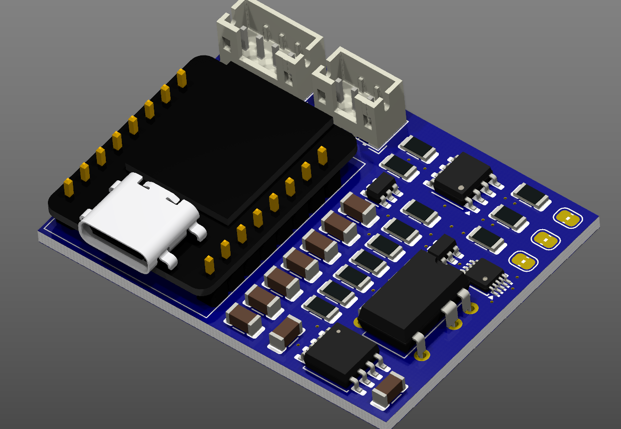
The image above shows a 3D rendering of one of my PCB designs. For me, this kind of view is always satisfying because it shows the design as an actual product-like object, not just a schematic. After starting from hand-drawn copper boards in 2011, seeing a clean 3D PCB model ready for fabrication is a reminder of how much the tools have changed — and how much fun the process still is.